poe@pcbamake.com


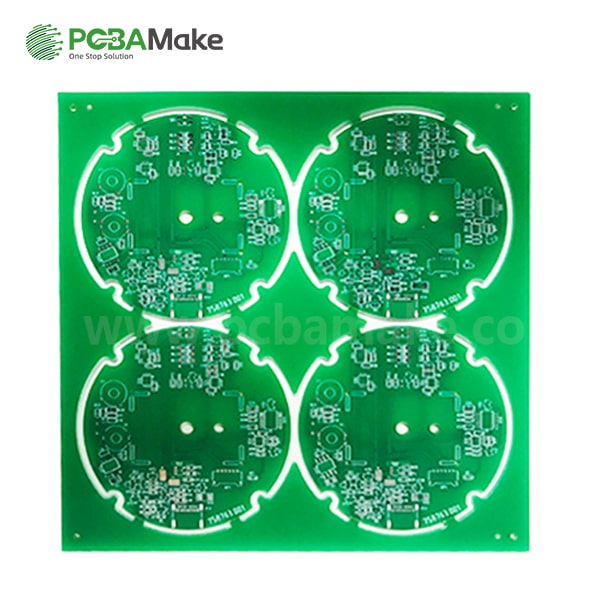


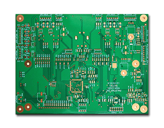
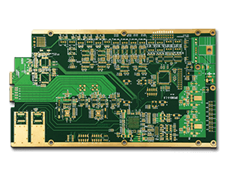
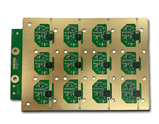
The double layer pcb solves the difficulty of the staggered of the wiring in the single -panel.
Material: FR4
Finish treatment: Immersion Gold
Copper thickness: 1oz~ 6oz
Resin plugging vias & Buried vias
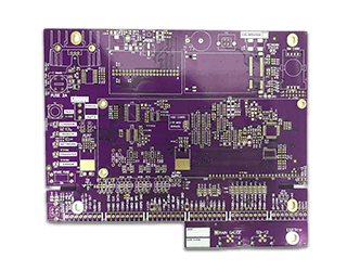
Impedance Controller Board
| Feature | Technical specification |
|---|---|
| Number of layers | 2 layer |
| Technology highlights | Epoxy glass dielectric materials laminated with copper cladding of varying thicknesses. |
| Copper Thickness: | 1OZ - 6OZ |
| Materials | FR4 |
| Copper weights (finished) | 18μm - 70μm |
| Minimum track and gap | 18μm - 210μm, advanced 1050μm / 30oz |
| PCB Finished Thickness | 0.40mm - 3.2mm |
| Maximum dimensions | 610mm x 450mm; dependent upon laser drilling machine |
| Surface finishes available | HASL (SnPb), LF HASL (SnNiCu), OSP, ENIG, Immersion tin, Immersion silver, Gold fingers |
| Minimum mechanical drill | 0.15mm |
| Minimum laser drill | 0.30mm standard, 0.20mm advanced |
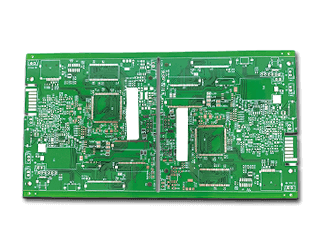
The double layer PCB is a board with double sided wiring on the board. An important feature of the double layer PCB is that it has guide holes to connect the wires on both sides into a circuit. The wiring of the double layer PCB can be interleaved, which is the biggest difference from the single-sided board; the double layer PCB is more suitable for complex circuits and has a wider range of use.
Double layer PCB is an extension of single sided. When single layer wiring cannot meet the needs of electronic products, double layer PCB is used. Both sides have copper cladding and traces, and the lines between the two layers can be conducted through vias to form the required network connections.
The double layer PCB solves the difficulty of the single sided board because of the staggered wiring.
Double layer PCB have many advantages, such as easy and simple wiring, less labor-intensive wiring, and shorter line lengths.
Delivery Services

Verified by

Link Us on