poe@pcbamake.com


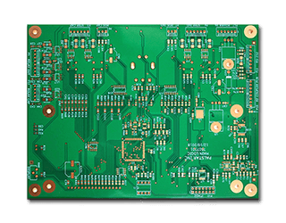
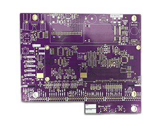
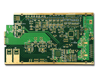
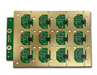
Multilayer PCB boards are suitable for complex devices with a large number of components and circuits in complex design.
Material: FR4,Polyimide,Aluminum,Teflon and others
Finish treatment: Immersion Gold
Copper thickness: 0.5oz~ 1oz
Surface Treatment: Immersion Gold/OSP/HASL
Solder Mask Color: Green/White/Blue/Red/purple/black
| Feature | Technical specification |
|---|---|
| Number of layers | 1 - 40 layers |
| Technology highlights | Multilayer boards with a higher connection pad density than standard boards, with finer lines/spaces, smaller via holes and capture pads allowing microvias to only penetrate select layers and also be placed in surface pads. |
| Silk Screen Color | White/Black |
| Materials | FR4 standard, FR4 high performance, Halogen free FR4, Rogers |
| Copper weights (finished) | 18μm - 70μm |
| Minimum track and gap | 0.075mm / 0.075mm |
| PCB thickness | 0.40mm - 3.20mm |
| Maximum dimensions | 610mm x 450mm; dependent upon laser drilling machine |
| Surface finishes available | OSP, ENIG, Immersion tin, Immersion silver, Gold fingers |
| Minimum mechanical drill | 0.15mm |
| Minimum laser drill | 0.10mm standard, 0.075mm advanced |
With the continuous innovation of electronic technology and the continuous improvement of the requirements for electronic equipment in some industries such as computers, medical treatment, and aviation, printed circuit boards are developing in the direction of smaller volume, lighter weight, and increased density. Single and double-sided printed boards can no longer meet the demand, so it is necessary to consider using more layers and higher assembly density multilayer circuit boards.
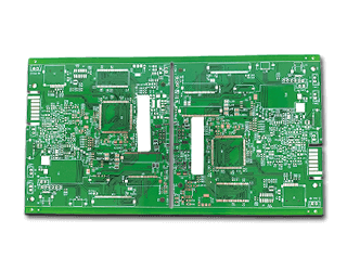
What is a multilayer circuit board?
In daily life, multilayer PCB circuit boards are currently the most widely used circuit board type. Multilayer PCB are circuit boards composed of two or more conductive layers (copper layers) superimposed on each other. The most common is four Six-layer board, such as the familiar computers in our daily life. Single-layer and double-layer boards are easy to distinguish and can be distinguished with the naked eye. Hold the board and look at the light. Except for the wiring on both sides, the rest of the place is transparent . But for multilayer PCB boards with four-layer boards and six-layer boards, if there is no corresponding mark on the board, it is not so easy to distinguish. Generally, the requirements for the structure design and process production of multilayer electric boards are very high, and the higher the number of layers, the more difficult it is, and it is suitable for use in more complex circuits.
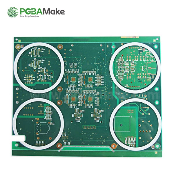
A typical multilayer PCB consists of the following parts:
Inner layer circuit board:The middle conductive layer, usually made of copper.
Insulation layer: The insulating material between the layers, usually epoxy or other high dielectric materials.
Surface circuit board: The outermost conductive layer used to connect external components.
Vias: The conductive path connecting the layers.
Multilayer PCB is widely used in various fields, especially in occasions where high performance and high density circuits are required.
Consumer electronics
Devices such as smart phones, tablets, and laptops rely on multilayer PCBs to achieve their complex functions and compact designs.
Communication equipment
Communication equipment such as routers, switches, and base stations need to process a large amount of data and signals, and multilayer PCBs can provide the required high reliability and high performance.
Medical equipment
Multilayer PCB is used in medical equipment for high-precision and high-reliability circuit design, such as MRI, CT scanners, and electrocardiographs.
Automotive electronics
Navigation systems, in-car entertainment systems, and advanced driver assistance systems (ADAS) in modern cars all rely on multilayer PCBs to achieve their complex functions.
Industrial control
Multilayer PCB is widely used in industrial automation and control systems, such as PLC (programmable logic controller), inverters, and robot controllers.
When designing and manufacturing multilayer PCBs, the following technical parameters are usually considered:
Number of layers: usually between 4 and 12 layers, and special applications may require more layers.
Board thickness: ranging from 0.4 mm to 3.2 mm.
Minimum line width/line spacing : usually between 0.1 mm and 0.2 mm.
Aperture: The diameter of the through hole is usually between 0.1 mm and 0.5 mm.
Material: FR4, ceramic, polyimide and other materials are commonly used.
Multilayer PCB has become an indispensable part of modern electronic devices with its high density, high performance and complex circuit design capabilities. Despite its high manufacturing cost and design complexity, its wide application in consumer electronics, communication equipment, medical equipment, automotive electronics and industrial control has fully demonstrated its value and importance. Through continuous technological innovation and optimization, multilayer PCB will continue to play an important role in the electronics industry.


Delivery Services

Verified by

Link Us on