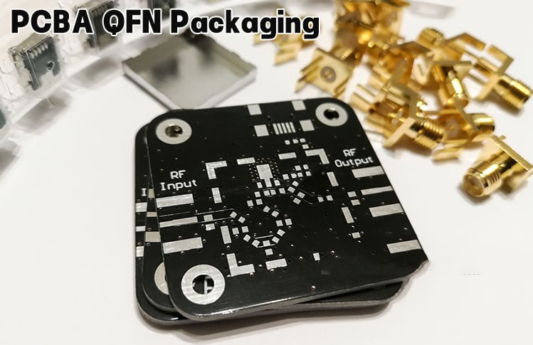
QFN Packaging in PCBA: Thermal Performance and Assembly Control
Quad Flat No-lead (QFN) packaging has become increasingly popular due to its compact size, excellent electrical performance, and superior thermal dissipation. However, these benefits come with strict assembly requirements.
How QFN packaging works and what PCBA manufacturers must control to ensure consistent quality.
Why QFN Is Widely Used
QFN packages feature:
No external leads
Exposed thermal pad on the bottom
Very short electrical connections

These characteristics result in:
Low parasitic inductance
Strong high-frequency performance
Efficient heat transfer into the PCB
Hidden Assembly Challenges of QFN
1. Bottom-Side Solder Joints
Since all solder joints are underneath the component:
Visual inspection is not possible
Solder joint quality must be verified by X-ray
This makes QFN assembly more complex than SOP or QFP packages.
2. Thermal Pad Soldering
The center thermal pad is critical for:
Heat dissipation
Mechanical stability
Improper solder paste volume can cause:
Excessive voiding
Component floating or tilting
Best practice is to use segmented stencil openings to balance solder volume and gas release.
3. Voiding Control
Excessive voids reduce thermal performance and reliability.
In most applications, voiding should be controlled below 25% of the thermal pad area.
PCBA Process Controls for QFN
Optimized stencil design for center pads
Controlled reflow profiles
X-ray inspection for void analysis
Stable PCB flatness and solder mask definition
QFN packaging rewards good process control—but exposes weaknesses very quickly.
Where QFN Packaging Performs Best
Power management ICs
RF and wireless modules
Industrial and automotive electronics

