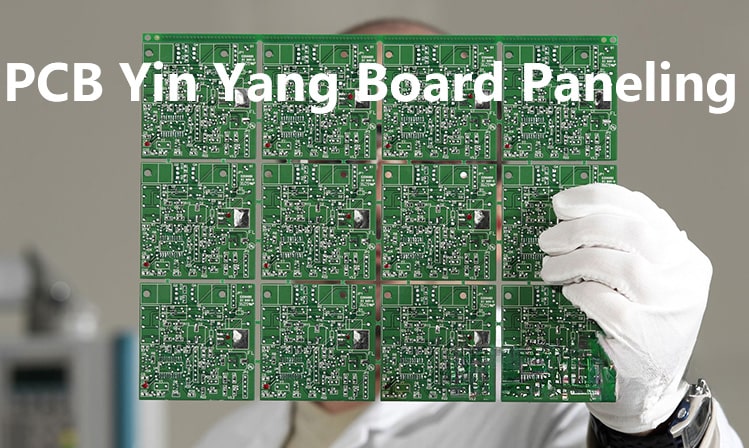
What are the advantages of Yin-Yang panel design in SMT patch processing?
Advantages and limitations of Yin-Yang panel design
In the electronics manufacturing industry, the design and manufacture of PCBs are crucial links. In order to improve production efficiency and reduce costs, manufacturers often use "Yin-Yang" panelization for production.

What is Yin-Yang panelization?
Yin-Yang panelization is a common PCB design technology used to optimize circuit layout, improve signal integrity and reduce interference. The basic principle of Yin-Yang panelization is to layout the signal and ground layers on different boards. Usually, the signal layer is placed on one board and the ground layer is placed on the other board. This layout can effectively reduce crosstalk and interference between signals while providing a good signal loop.
Advantages and limitations of Yin-Yang panel design in SMT patch processing
Advantages
1. Improve production efficiency
Reduce production time: Yin-Yang panel design can produce multiple PCBs in one manufacturing process, thereby significantly reducing the production time of a single board.
Reduce the frequency of line change and equipment adjustment: By processing multiple PCBs at one time, the number of line change and equipment adjustment on the production line is greatly reduced, improving overall production efficiency.
2. Reduce costs
Reduce the waste of raw materials: The panel design can make more efficient use of the board and reduce the waste of scraps.
Unit cost reduction: Due to the improvement of production efficiency, the manufacturing cost of the unit PCB can be reduced, thus saving a lot of costs in mass production.
3. Facilitate testing and quality control
Simultaneous detection of multiple circuits: The panel design allows multiple circuit boards to be tested at the same time, so as to quickly troubleshoot problems and improve testing efficiency and quality control capabilities.
Limitations
1. Increased design difficulty
Accuracy of electrical connections: The Yin-Yang panel design needs to ensure the accuracy of all electrical connections, and requires complex layout planning to take into account the utilization of the board and the feasibility of manufacturing.
2. Increased manufacturing difficulty
Welding stress problem: The thermal expansion coefficients of different boards may be different, which is easy to cause stress problems during the welding process, affecting the reliability of the product.
3. Difficulty in repair and rework
Local problems are difficult to solve: Once a problem occurs in a certain part of the panel, the entire board may need to be replaced, which increases the difficulty and cost of repair and rework.
Time-consuming problem location: Problem location and repair of large panels are time-consuming and labor-intensive, which is not conducive to rapid response and problem solving.
4. Limited flexibility
High cost of design changes: Changing a panel design may require redesigning the entire board, increasing the cost and time of changes.
Limited scope of application: Not all types of PCBs are suitable for Yin-Yang board design, especially for complex PCBs with extremely high wiring density and precision requirements and situations with stringent signal integrity requirements, Yin-Yang board design may have adverse effects.
Applicable conditions and restrictions
For PCBs in some special application scenarios, such as circuits with very high signal integrity requirements, Yin-Yang board design may introduce some adverse effects. In addition, different manufacturing processes and equipment conditions will also affect the feasibility of Yin-Yang board design.
If you need to know more about PCB proofing, SMT patch, PCBA processing related technical knowledge, please leave a message to get it!

