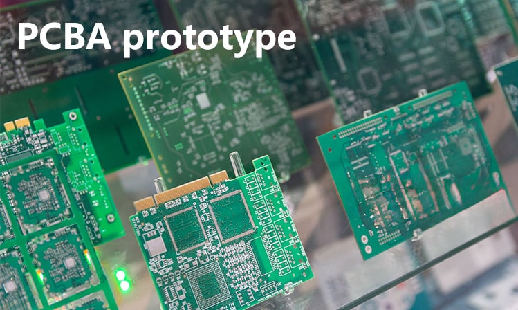
What are the necessary processes for PCBA proofing?
Key processes and key points of PCBA proofing
In the electronic equipment manufacturing industry, PCBA proofing is a crucial link. It is not only a preliminary verification of product research and development, but also the basis for ensuring the quality and stability of the final product.
Key processes and key points of PCBA proofing
1. Circuit board design and review
The first step of PCBA proofing is circuit board design. This is usually completed by electronic engineers using professional electronic design automation (EDA) tools. The design stage needs to consider multiple aspects such as circuit layout, component arrangement, signal integrity, and power distribution. After the design is completed, a strict review must be conducted to ensure the rationality and feasibility of the circuit design.

Key points of design review:
1. Whether the layout of the power supply and ground wires is reasonable: whether there is a potential risk of short circuit or open circuit.
2. Whether the spacing between components meets the production process requirements: to avoid problems such as bridging or cold soldering during the production process.
3. Whether the direction and length of the signal line are reasonable: to reduce signal interference and attenuation.
2. Material selection and procurement
After the design review is passed, the next step is to select and purchase the required materials. This includes circuit board substrates, electronic components, pads, connectors, etc. The choice of materials has a crucial impact on the stability and reliability of PCBA prototype.
Material selection points:
Main points for processing and welding:
Functional test and verification content:
5. Problem location and modification
If problems are found during the test, problem location and modification are required. This stage is crucial to ensure the final quality of the circuit board.
Problem location and modification points:
Aging test content:
After the aging test is completed, final verification is required. This stage mainly conducts comprehensive functional and performance tests on the circuit board to ensure that it meets the design requirements and has stable performance.
The PCBA proofing process involves multiple key links, from design review to material selection, to processing and welding, functional testing and verification, problem location and modification, and aging testing and final verification. Each link is crucial and cannot be ignored. As a purchaser of an electronic equipment manufacturer, understanding and mastering these processes is of great significance to ensuring the stability and reliability of the circuit board.
If you have PCB/PCBA/OEM/ODM needs, please contact us, We will reply within 2 hours, and complete the quotation within 4 hours or less upon request.