Comparison of SMT and DIP processes
In the field of PCBA (printed circuit board assembly) manufacturing, surface mount technology (SMT) and dual in-line package technology (DIP) are the two most mainstream assembly processes.

1. SMT and DIP processes
1. Surface mount technology (SMT)
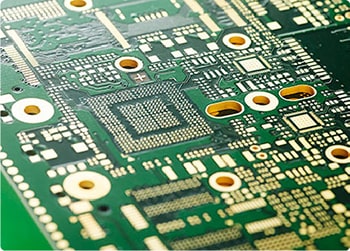
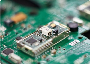
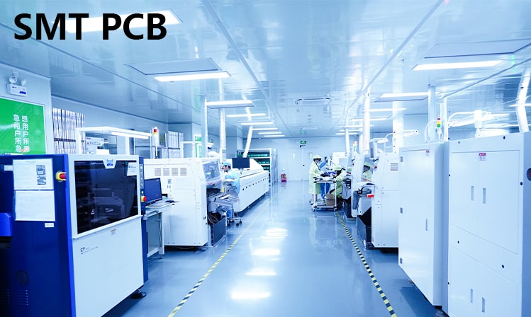
SMT (Surface Mount Technology) is an assembly technology that directly mounts electronic components to the surface of a PCB. Components are usually pinless or short-pin designs and are fixed to the PCB by soldering with solder paste.
Main features:
Miniaturization and high density of components
High degree of automation
Suitable for mass production
Relatively low soldering temperature
2. Dual in-line package (DIP)
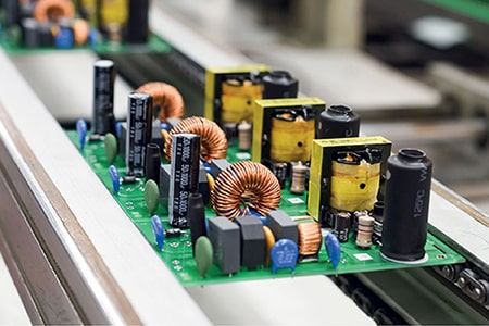
DIP (Dual In-line Package) is a traditional assembly technology. Components have long pins and need to be inserted into PCB through-holes for soldering.
Main features:
Large component size
High mechanical strength
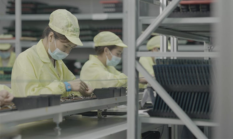
Suitable for manual operation and maintenance
Higher soldering temperature
II. Comparison of process details
Comparison items SMT process DIP process
Component type Surface mount device (SMD) Through-hole device (THD)
Assembly density High (double-sided mounting can achieve higher density) Low (limited by pin spacing and size)
Process flow Printing solder paste → SMD → Reflow → Inspection Plug-in → Wave soldering → Cut pins → Inspection
Automation level Fully automated (up to 99% or more) Semi-automated (partial manual plug-in required)
Production speed Fast (tens of thousands of points per hour) Slow (hundreds to thousands of points per hour)
Initial investment High (special equipment required) Low (relatively simple equipment)
III. Comparison of performance and reliability
1. Electrical performance
SMT advantages: small parasitic inductance and capacitance, good high-frequency characteristics, fast signal transmission speed
DIP limitations: longer pins lead to larger parasitic parameters, limited high-frequency performance
2. Mechanical strength
DIP advantages: high mechanical strength of through-hole soldering, strong resistance to vibration and impact
SMT limitations: solder joints directly bear mechanical stress, low reliability in extreme environments
3. Thermal management
SMT advantages: large contact area between components and PCB, good heat dissipation performance
DIP features: some high-power components can dissipate heat through pins, high design flexibility
4. Difficulty of maintenance
DIP advantages: easy replacement of components, suitable for prototype development and maintenance
SMT challenges: professional rework equipment is required, and multi-pin components are difficult to rework
IV. Cost-benefit analysis
1. Production cost
SMT: The cost of mass production is extremely low, but the equipment depreciation and maintenance costs are high
DIP: small batch production is flexible and economical, but the labor cost accounts for a high proportion
2. Material cost
SMT: component cost is generally low (miniaturization), but PCB design requirements are high
DIP: some special components have higher costs, but PCB requirements are relatively simple
3. Comprehensive cost
Production volume <1000: DIP may be more economical
Production volume 1000-10000: Specific analysis is required
Production volume >10000: SMT has obvious cost advantages
V. Application scenario recommendations
Situations where SMT is preferred:
Consumer electronics (mobile phones, tablets, etc.)
High-frequency circuit design
Miniaturized equipment
Large-scale standardized production
Weight-sensitive applications

Situations where DIP is preferred:
High-power electronic equipment
Industrial/military products with high reliability requirements
Development boards for education/experiments
Small-scale multi-variety production
Required Scenarios of frequent component replacement
VI. Industry development trends
SMT's dominant position is consolidated: With the trend of component miniaturization, SMT's market share continues to expand
Hybrid technology application: high-end products often use SMT+DIP hybrid process
DIP special field adherence: high-power and high-reliability fields are still indispensable
New packaging technology: BGA, QFN and other packaging forms promote SMT process innovation
Intelligent upgrade: AOI, SPI and other detection technologies are deeply integrated with SMT
VII. Conclusion
SMT and DIP have their own advantages and disadvantages, and there is no absolute distinction between good and bad. PCBA manufacturers should reasonably choose assembly processes based on product characteristics, production scale, cost budget and reliability requirements. For most modern electronic products, a hybrid assembly strategy with SMT as the main and DIP as the auxiliary is often the best choice. With the advancement of technology, the two processes are also constantly integrating and developing, jointly promoting the electronic manufacturing industry to move forward.

