The difference between DFM and DFA in the PCB industry
DFM (Design for Manufacturability) and DFA (Design for Assembly) are two key concepts. The two seem similar, but they focus on different points in actual applications.
What is DFM?
DFM (Design for Manufacturing) refers to fully considering the limitations and requirements of the manufacturing process during the design phase, optimizing the design to improve production efficiency and reduce manufacturing costs. Its core goal is to ensure that the PCB design can be produced efficiently and reliably while reducing potential problems in the manufacturing process.

DFM Focus
Material selection: Ensure that the PCB material (such as copper foil, insulation layer) is suitable for the expected manufacturing process and meets the performance requirements of the product.
Board layer design: Optimize the stacking structure of multi-layer boards to avoid signal interference and abnormal electrical performance.
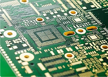
Aperture and spacing: Design reasonable via size, pad spacing and wiring width to adapt to the capabilities of manufacturing equipment.
Processing tolerance: Consider manufacturing tolerances and deviations to avoid production difficulties due to overly precise designs.
Testability: Add test points to the design to facilitate electrical testing in the production phase.
What is DFA?
DFA (Design for Assembly) refers to optimizing the layout and structure of PCB during the design phase to facilitate subsequent assembly processes (such as soldering components, patching, etc.). The core of DFA is to improve assembly efficiency, reduce errors and rework in assembly, and ensure product reliability.
DFA Focus
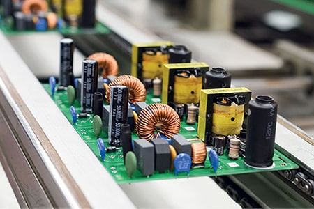
Component Layout: Arrange the positions of components reasonably to avoid interference between components and ensure that there is enough space for soldering or patching.
Welding Process: Optimize pad design (such as shape, size and spacing) to adapt to different soldering processes such as wave soldering and reflow soldering.
Operability: Ensure that components are easy to install and maintain, such as avoiding too dense layout or difficult-to-reach solder joints.
Directional Uniformity: Try to make the directions of components of the same type consistent to reduce the complexity of the assembly process.
Mechanical Fixation: For components that require additional mechanical support (such as large-volume capacitors or connectors), design a reasonable fixing structure.
The main difference between DFM and DFA
DFM (Design for Manufacturing) focuses on the manufacturing process of PCB, optimizes the design to adapt to the production capacity of the factory, improves efficiency and reduces manufacturing costs, focusing on material selection, processing tolerance and board layer design.
DFA (Design for Assembly) focuses on the assembly process of PCB, optimizes component layout and pad design, improves assembly efficiency and reduces errors, focusing on component layout, welding adaptability and maintainability.
Simply put, DFM solves "how to manufacture circuit boards" and DFA solves "how to efficiently assemble circuit boards". The combination of the two ensures the efficiency and reliability of products from design to mass production.
The relationship between DFM and DFA
Although DFM and DFA are two independent concepts, they are inseparable in practical applications. An excellent PCB design needs to take into account the requirements of DFM and DFA at the same time:
Design stage: Design engineers need to comprehensively consider the constraints of manufacturing and assembly and balance the needs between the two. For example, overly complex wiring or too high assembly density may have a negative impact on both manufacturing and assembly.
Collaboration link: Feedback from PCB manufacturing plants and electronic assembly plants is very important for optimizing DFM and DFA. Through the collaboration between the two parties, potential problems can be discovered and solved.
Why are DFM and DFA so important?
In the modern electronic manufacturing industry, product development cycles are getting shorter and shorter, and market competition is becoming increasingly fierce. As an indispensable part of PCB design, DFM and DFA can bring the following advantages:
Reduce costs: Reduce problems in manufacturing and assembly through optimized design, thereby reducing scrap rate and rework costs.
Shorten cycle: Reduce rework time caused by design defects and speed up product launch.
Improve quality: Ensure that PCBs are more reliable during manufacturing and assembly, and ultimately improve the overall quality of the product.
Improve efficiency: Through reasonable design, improve the degree of automation of production and assembly, and reduce manual intervention.
Although DFM and DFA have different focuses in PCB design, they work together in the manufacturing and assembly links of products and are the key to achieving high-quality and efficient production.

