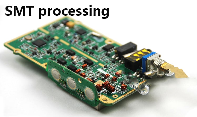
What is the difference between AOI and SPI detection technology in SMT processing?
The importance of AOI and SPI in SMT processingIn the electronics manufacturing industry, the accuracy and quality of SMT processing directly affect the performance and reliability of the product. In order to ensure the high-quality production of electronic products, AOI (automatic optical inspection) and SPI (solder paste inspection) technologies have become the core detection methods of SMT production lines.
1. SPI (Solder Paste Inspection) Technology: Precise Control of Welding Basics

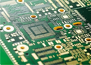
Definition and Principle of SPISPI (Solder Paste Inspection) is an automated device for detecting parameters such as thickness, area and volume of solder paste printed on PCB boards. Through laser, optical or 3D imaging technology, the SPI system can detect the quality of solder paste on PCB pads in real time to ensure that each solder joint has ideal welding conditions.
Application Scenarios of SPIPCB solder paste printing inspection: Ensure that the solder paste on the pad is uniform and of moderate thickness to avoid excessive or insufficient solder joints or short circuits.
Quality control before component welding: Provide reliable data reference for the mounting process to reduce the defect rate.
Advantages of SPI
Improve welding reliability: welding defects are mostly caused by poor solder paste printing. SPI can detect problems in advance and reduce scrap rate.
Reduce rework costs: real-time detection and correction to avoid welding failures in subsequent production.
Improve production efficiency: optimize solder paste printing process and improve the stability of SMT production line.
2. AOI (Automated Optical Inspection) Technology: Intelligent Quality Assurance
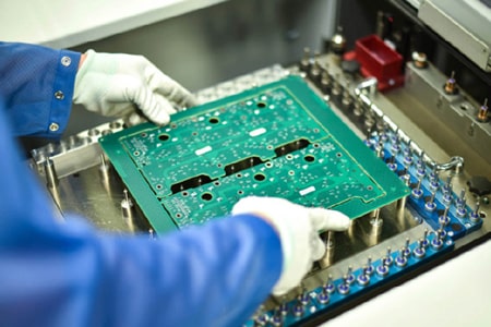
Definition and Principle of AOIAOI (Automated Optical Inspection) is to inspect the mounted PCB through high-resolution cameras and image processing algorithms. By comparing the image of the PCB with the standard template, the system can automatically identify the missing, misaligned, polarity errors and welding defects of components.
Application Scenarios of AOI
Post-SMT inspection: detect the assembly quality of components such as position, angle, polarity, etc.
Post-Reflow inspection: check the quality of solder joints and identify welding defects such as cold soldering and bridging.
Advantages of AOI
High detection accuracy: solder joint defects and device misalignment as small as micron level can be detected.
Fully automated process: no manual intervention is required, the detection speed is fast, and it is suitable for mass production.
Production traceability and data analysis: the detection results can be saved and tracked, supporting production data analysis and quality improvement.
3. The importance of AOI and SPI in SMT processing
In SMT processing, AOI and SPI together constitute a complete quality control system:
Preliminary prevention: SPI detects the quality of solder paste printing to avoid basic welding problems.
Process control: AOI monitors the mounting and welding processes in real time to detect assembly and welding defects.
Quality improvement: Double detection greatly reduces the rework rate and improves the reliability and customer satisfaction of finished products.
By deeply integrating these two technologies into the SMT production line, electronic manufacturers can achieve the goal of zero defects, comprehensively improve the efficiency and yield rate of the production line, and thus enhance market competitiveness.
Follow PCBAMake. If you need to know more about PCBA proofing, PCBA OEM, and PCBA processing related technical knowledge, please leave a message to get it!

